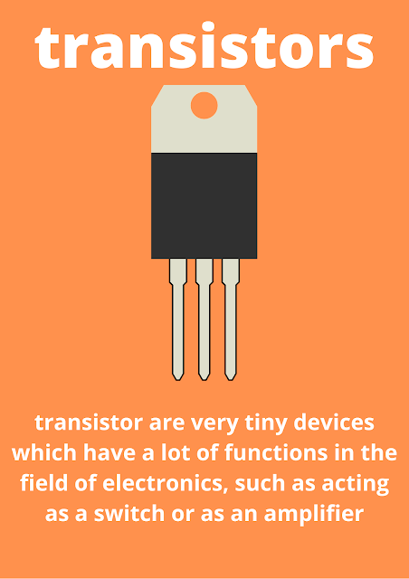
Transistors are present almost every electronic equipment that you come across in your day to day life
There are nearly 100 million transistors in a mobile phone and nearly over 1 billion transistors are present on a laptop or a personal computer
in this article, we will be dealing with the following topics
- what is transistor
- science of semiconductors
- n-type doping
- p-type doping
- working of a transistor
- transistor as a switch
- transistor as an amplifier
What is transistor
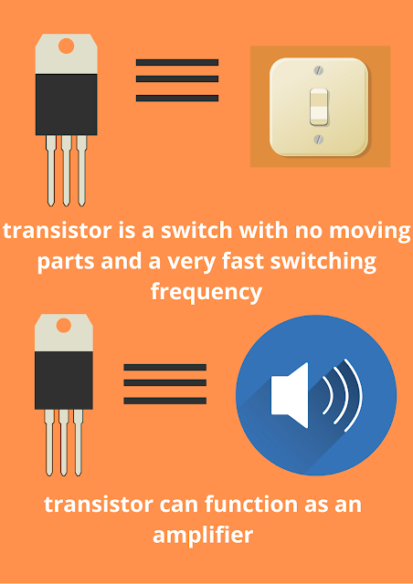
Transistors in its simplest form can be thought off as a switch with special features
The mechanical switch can control the flow of electric current and can be turned on and off
Likewise, the same thing can be done with a transistor
Unlike a mechanical switch, a transistor does not have any moving parts, does not need any human operator and can operate at a very fast rate
Transistors are do all this because of the advancements in the science of semiconductors
Science of semiconductors
Semiconductors, as clear by their name, are materials which can conduct electricity, but not as efficiently as conductors
They don’t exactly oppose the conduction of electricity(like insulators), hence they are classified as semiconductors
In a silicon semiconductor (denoted bu Si), the silicon atoms form 4 covalent bonds with their neighboring atoms in the lattice
Whenever any of the electrons present in the covalent bonds get some energy from external sources, they leave the bond and Rome around in the lattice
This is the reason for the conduction of semiconductor materials
This conductivity of semiconductors can be increased by dopping them with suitable material
Semiconductors Doping means the addition of another material in a natural semiconductor to increase its conductivity
There are essentially 2 types of semiconductor doping-
1 n-type doping -
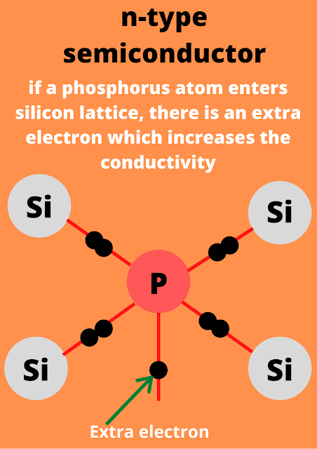
Whenever an atom of material with more number of electrons enters the semiconductor lattice, there are extra electrons, which increases the conductivity
For example
If a phosphorus atom(which has 5 electrons to make bonds) enters in silicon(which need only 4 electrons to make bonds) lattice
Now phosphorus has 5 bond making electrons, but silicon requires only 4 electrons to make bonds
Hence there is the presence of an extra electron
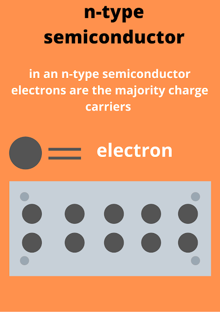
And there will be many such electrons in the entire semiconductor lattice, increasing conductivity
Here the conductivity increases due to electrons, which have a negative charge, hence the name n-type doping
2 P-type doping -
p-type doping is simply the opposite of n-type doping
In p-type doping, such an atom enters the semiconductor lattice which has a lesser number of electrons than that required to form bonds
For example-
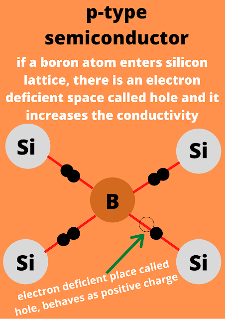
If a boron atom(which has 3 electrons to make bonds), enters silicon(which require 4 electrons to form bonds) lattice, there will be a shortage of electrons
Now boron only has 3 bond making electrons and silicon requires 4 electrons to make bonds
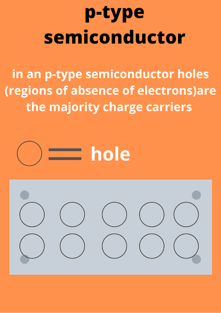
Hence, there will be an absence of electrons (known as holes) creating the effect of positive charge
Here the conductivity increases due to holes (behaving as positive charges), which can be thought of as positive charges, hence the name p-type doping
how does a Transistor works-
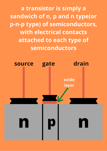
A transistor is made by the combinations of the n-type and p-type semiconductors
A transistor is essentially a combination of 3 layers of semiconductors
A transistor made by the combination of a p-type layer sandwiched in between 2 n-type semiconductors is known as npn transistors
And, a transistor made with an n-type semiconductor sandwiched between 2 p-type semiconductors is called a pnp transistor
Apart from these 3 semiconductor layers, transistors have 2 terminals from the electrical contacts at the 2 n-type semiconductor layers
And an additional terminal is present, which is insulated from the transistor by an oxide layer known as the gate
transistor as a switch-
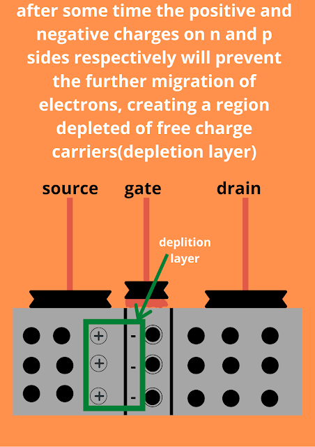
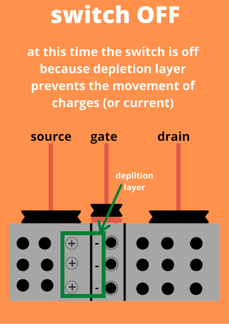
When the n-type and the p-type semiconductors are fused together, electrons from the n-type semiconductor move towards the p-type semiconductor (to fill up the holes)
And after some time p-type semiconductors become negatively charged (due to electrons from the p-type semiconductor), creating a barrier for further electrons from p-type semiconductor (since electrons repel each other)
When the holes in p-type are filled by excess electrons from p-type, a region called depletion layer is created
The depletion layer is called so because there are no excess electrons or holes to cause conduction
This depletion region blocks the conduction of electrical current, hence the switch is in the off state
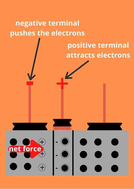
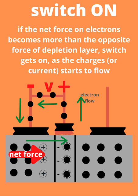
To turn on the switch we need to provide a small positive voltage at the gate terminal
This positive voltage will help the electrons in n-type semiconductors to cross the depletion layer, hence conduction will start
Thus this positive voltage nullifies the effect of deception layer ( which keeps the switch in the off state), turning the switch on
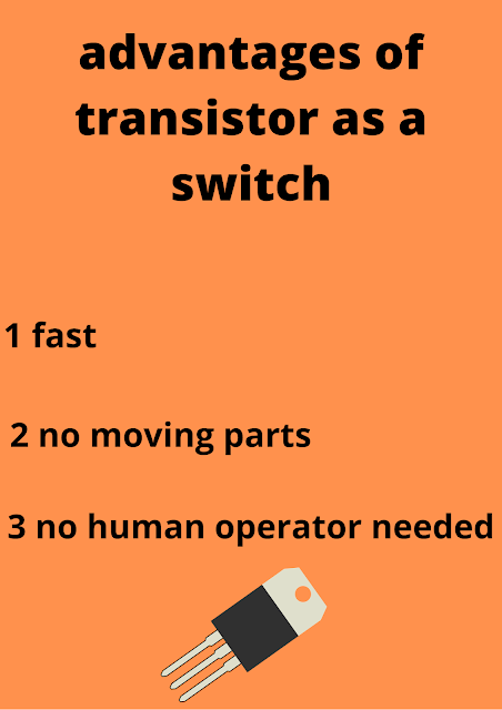
Advantages of transistors as a switch-
1 transistors are very fast switches-
As seen above that switching a transistor on or off depends upon the value of the voltage applied at the gate of the transistor
A voltage can certainly do switching at a very fast rate when compared to a human operating a mechanical switch
2- no moving parts-
As seen above that transistor acting as a switch, but unlike a mechanical switch it didn’t have any moving parts
Absence of moving parts is always better, as strength lies in unity
Transistor as an amplifier-
Second (and probably the most well known) application of transistor is as an amplifier
While giving a positive voltage at the gate terminal (which switches the transistor on), we apply another voltage between the source and drain
Now the electrons in the n region are attracted by 2 voltages
1the one applied between the gate and source terminal
2 the one which is applied in between the source and the drain terminal
Due to this excess positive voltage, the majority of electrons in the n-type semiconductors pass the p-type semiconductor and reaches the other end
While at the same time electrons are also flowing between source and gate
Thus we have the following conclusions-
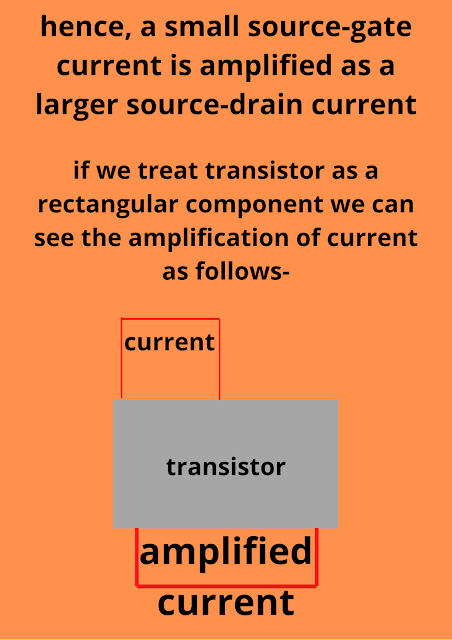
Electrons flowing from source to gate are very less as compared to those flowing in between the source and drain
Thus source-drain current is very large as compared to the source-gate current
Hence, the current is amplified!
In other words, if we give an audio signal at the source-gate region and a speaker at the source-drain region, we will hear am amplified sound
Conclusion-
Which was the most interesting thing you got to learn about transistors in this article
Or do you have any doubt regarding anything?
Either way, you can leave a comment to let us know about it, so go ahead and comment



Comments
Post a Comment